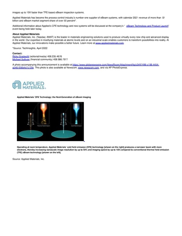
images up to 10X faster than TFE-based eBeam inspection systems. Applied Materials has become the process control industry’s number-one supplier of eBeam systems, with calendar 2021 revenue of more than $1 billion and eBeam market segment share of over 50 percent*. Additional information about Applied’s CFE technology and new systems will be discussed at the company’s “ eBeam Technology and Product Launch” event being held later today. About Applied Materials Applied Materials, Inc. (Nasdaq: AMAT) is the leader in materials engineering solutions used to produce virtually every new chip and advanced display in the world. Our expertise in modifying materials at atomic levels and on an industrial scale enables customers to transform possibilities into reality. At Applied Materials, our innovations make possible a better future. Learn more at www.appliedmaterials.com. *Source: TechInsights, April 2022 Contact: Ricky Gradwohl (editorial/media) 408.235.4676 Michael Sullivan (financial community) 408.986.7977 A photo accompanying this announcement is available at https://www.globenewswire.com/NewsRoom/AttachmentNg/c3497496-c198-4454- a546-056b4d7c72fd. This photo is also available at Newscom, www.newscom.com, and via AP PhotoExpress. Applied Materials’ CFE Technology: the Next-Generation of eBeam Imaging Operating at room temperature, Applied Materials’ cold field emission (CFE) technology [shown on the right] produces a narrower beam with more electrons, thereby increasing nanoscale image resolution by up to 50% and imaging speed by up to 10X compared to conventional thermal field emission (TFE) eBeam technology [shown on the left]. Source: Applied Materials, Inc.
 Applied Materials Breakthrough in Electron Beam Imaging Technology Accelerates Development of the World’s Most Advanced Computer Chips Page 1