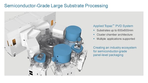
Semiconductor-Grade Large Substrate Processing ™ Applied Topaz PVD System Substrates up to 600x600mm Cluster chamber architecture Multiple applications supported Creating an industry ecosystem for semiconductor-grade panel-level packaging
 Upload and Go Page 48 Page 50